Production and Application of PCB Antenna Manufacturers
Introduction
PCB antennas are an essential component of wireless communication systems. They are used to send and receive signals in applications such as mobile phones, routers, and other wireless devices. Antennas have a significant impact on the performance and efficiency of a wireless system. In this article, we will explore the design and manufacturing process of PCB antennas.
Types of PCB Antennas
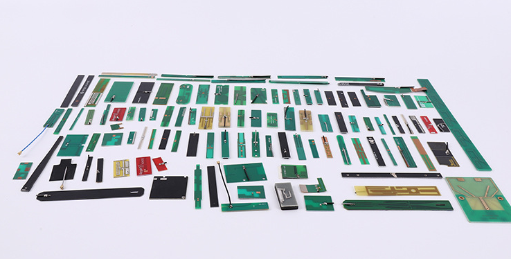
There are several types of PCB antennas used in different applications. Some of the most common types of PCB antennas are:
1. Microstrip Antennas – Microstrip antennas, also known as patch antennas, are widely used in wireless communication systems. These antennas are thin, flat, and can be easily integrated into electronic devices.
2. Planar Inverted-F Antennas (PIFA) – Planar inverted-F antennas are commonly used in mobile phones due to their compact size and low profile.
3. Monopole Antennas – Monopole antennas are vertically oriented and may require a ground plane to function properly. These antennas are commonly used in wireless routers and access points.
Design Considerations
The design of a PCB antenna is critical for optimal performance. There are several design considerations that need to be taken into account during the design process. Some key design considerations are:
1. Antenna dimensions – The size of the antenna is critical in determining the operating frequency and bandwidth of the antenna.
2. Antenna shape – The shape of the antenna affects the radiation pattern and impedance characteristics of the antenna.
3. Antenna placement – The placement of the antenna within the electronic device is critical in optimizing the radiation pattern and minimizing interference.
4. Substrate – The substrate material and thickness affect the performance and efficiency of the antenna.
Manufacturing process
The manufacturing process of PCB antennas involves several steps. The process can vary greatly depending on the type of antenna and the manufacturing capabilities of the PCB antenna manufacturer. However, the basic steps involved in manufacturing a PCB antenna are:
1. Design – The design of the antenna is created using computer-aided design (CAD) software.
2. Substrate Preparation – The substrate material is prepared in accordance with the design specifications.
3. Deposition of Metal – The metal layer is deposited onto the substrate using various techniques such as sputtering or evaporation.
4. Photolithography – The metal layer is then patterned using photolithography techniques to create the desired antenna shape.
5. Etching – The metal layer is etched to remove unwanted metal and create the final antenna shape.
6. Testing – The antenna is then tested to ensure that it meets the design specifications.
Conclusion
In conclusion, PCB antennas are a crucial component of wireless communication systems. A well-designed PCB antenna can significantly improve the performance and efficiency of the wireless system. The design and manufacturing process of PCB antennas involve several critical design considerations and manufacturing steps. Understanding the design and manufacturing process is essential for selecting the right PCB antenna and ensuring optimal performance.
